Base Materials for PWBs
Halogen Free, High Tg, High Elastic Modulus, Low CTE Multilayer Material – MCL-E-770G (Type R)
Product Information and Application
Product form
- CCL: MCL-E-770G (Type R)
- Prepreg; GEA-770G
Applications
- Semiconductor packages. (FC-CSP, PoP, SiP)
- Thinner module.
Features
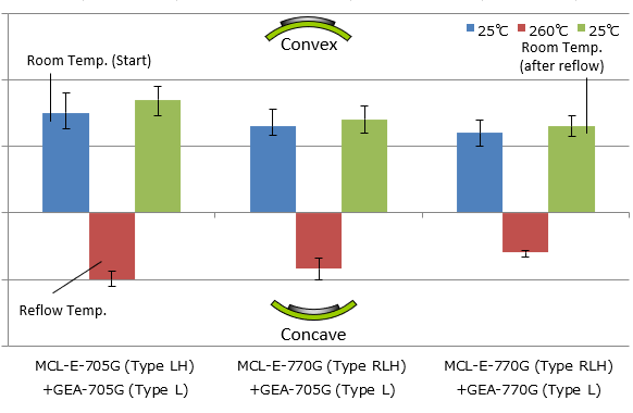
- MCL-E-770G has low CTE values in X, Y directions and reduces warpage of package substrate significantly.
- MCL-E-770G (Type RLH) has lower CTE value (less than 2.0ppm/℃).
Characteristics
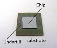
Warpage of FC-CSP

TEG Chip
- Chip size: 7.3mm×7.3mm
- Chip thickness: 150 µm
- Underfill thickness: 60 µm (CEL-C-3730-4)
- Solder Resist thickness: 20 µm (FZ-2700GA)
TEG Substrate
- Package size: 14mm×14mm
- Core Thickness 200 µm+1024 (S-HD) PPG

Thin Laminate
| Item | Condition *3 | Unit | Actual Value | Reference (IPC-TM-650) |
||
|---|---|---|---|---|---|---|
| MCL-E- 770G (Type R) |
MCL-E- 770G (Type RLH) |
|||||
| Tg | TMA method | A | ℃ | 260–280 | 2.4.24 | |
| DMA method | A | 300–330 | ‐ | |||
| CTE *1 | X (30–120℃) | A | ppm/℃ | 4.0–6.0 | 1.5–2.0 | ‐ |
| Y (30–120℃) | 4.0–6.0 | 1.5–2.0 | ||||
| Solder Heat Resistance (260℃) | A | sec. | >300 | ‐ | ||
| T260 (Without copper) | A | min. | >60 | 2.4.24.1 | ||
| T288 (Without copper) | >60 | |||||
| Decomposition Temperature (TGA method 5% Weight Loss) | A | ℃ | 430–450 | 2.3.40 | ||
| Heat Resistance for HDI Process (Semi-Additive) | 260℃ Reflow | cycles | >20 | ‐ | ||
| Copper Peel Strength | 12 µm | A | kN/m | 0.7–0.9 | 2.4.8 | |
| 18 µm | 0.8–1.0 | |||||
| Surface Roughness (Ra) | A | µm | 2–3 | 2.2.17 | ||
| Flexural Modulus (Lengthwise) *4 | A | GPa | 30–32 | 34–36 | ‐ | |
| Dielectric Constant | 10GHz *2 | A | - | 4.2–4.4 | 3.9–4.1 | IEC-61189-2-721 |
| Dissipation Factor | 10GHz *2 | A | - | 0.006–0.008 | 0.006–0.008 | IEC-61189-2-721 |
| Volume Resistivity | C-96/40/90 | Ω・cm | 1×10¹⁴–1×10¹⁶ | 2.5.17 | ||
| Surface Resistance | C-96/40/90 | Ω | 1×10¹³–1×10¹⁵ | |||
| Insulation Resistance | A | Ω | 1×10¹⁴–1×10¹⁶ | ‐ | ||
| D-2/100 | 1×10¹²–1×10¹⁴ | ‐ | ||||
*1) Heating Rate: 10℃/min., *2) Measured by SPDR., *3) Refer to “Condition Note“, *4) t0.8mm
t0.4mm thickness core is used depending on test item.
*Above data are experimental results and not guaranteed.
Standard Specifications
Copper Clad Laminate
| Part Number | Type | Copper Foil Thickness | Code Name | Laminate Thickness |
|---|---|---|---|---|
| MCL-E-770G | (R) | 2 µm 3 µm 12 µm (LP, PF) |
T0.05 | 0.05mm |
| U0.04 | 0.04mm | |||
| 2 µm 3 µm 12 µm (STD, LP, PF) |
M0.06 | 0.06mm | ||
| 0.1 | 0.11mm | |||
| HD0.15 | 0.16mm | |||
| 0.2 | 0.21mm | |||
| (RLH) | 2 µm 3 µm 12 µm 18 µm (STD, LP, PF) |
U0.04 | 0.04mm | |
| M0.06 | 0.06mm | |||
| 0.1 | 0.11mm | |||
| D0.15 | 0.16mm | |||
| 0.31 | 0.31mm |
Note1) STD: Standard copper foil, LP: Low profile copper foil, PF: Profile free copper foil.
Note2) STD: 12 µm, 18 µm; LP: 2 µm, 3 µm, 12 µm, 18 µm.
Note3) In case laminate thickness lies in between two thickness figures shown above, the tolerance of such laminate would be equal to the tolerance of the thicker one.
Note4) The thickness means that of dielectric layer.
Prepreg
| Part Number | Type | Glass Cloth | Properties | |||
|---|---|---|---|---|---|---|
| Style | Resin Content (%) |
Dielectric Thickness after Lamination *1 (mm) |
||||
| GEA-770G | (F) | ≦0.025 | (See [GEA-770G (Type F)] page for ultra thin, flat prepregs) | |||
| ‐ | 0.025 | (1017N72) | 1017 | 72±2 | 0.025 | |
| 0.025 | (1017N76) | 1017 | 76±2 | 0.030 | ||
| 0.03 | (1027N72) | 1027 | 72±2 | 0.040 | ||
| 0.03 | (1027N76) | 1027 | 76±2 | 0.048 | ||
| 0.04 | (1037N72) | 1037 | 72±2 | 0.048 | ||
| (L) | 0.025 | (L1017N72) | 1017 | 72±2 | 0.025 | |
| 0.025 | (L1017N76) | 1017 | 76±2 | 0.030 | ||
| 0.03 | (L1027N72) | 1027 | 72±2 | 0.040 | ||
| 0.03 | (L1027N76) | 1027 | 76±2 | 0.048 | ||
| 0.035 | (L1024N68) | 1024 | 68±2 | 0.041 | ||
| 0.035 | (L1024N73) | 1024 | 73±2 | 0.050 | ||
| 0.04 | (L1037N72) | 1037 | 72±2 | 0.048 | ||
| 0.045 | (L1030N71) | 1030 | 71±2 | 0.058 | ||
| Reference (IPC-TM-650) | 2.3.16 | ‐ | ||||
*1) The dielectric thickness after lamination is defined as the thickness of one sheet of prepreg when the resin flow is 0%.
This value changes depending on the press condition or inner layer pattern.
