Photosensitive Materials for PWBs
PV-F Series
Product Information
PV-F series are film type photosensitive materials to form pattern for high density wiring interposer and build-up layer.
Features
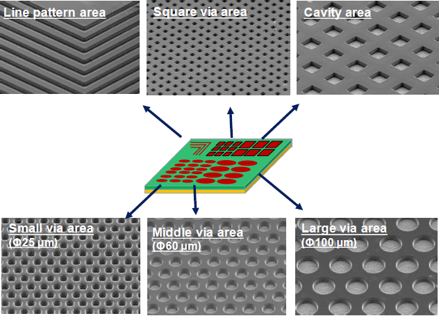
- This material forms square and via patterns by applying the photolithography process (exposure, development), can support the improvement of the design margin of semiconductor PKG substrate.
- This material forms a seed layer by electroless plating by applying desmear process
(One of our data)
| Item | Unit | PV-F008 |
|---|---|---|
| Seeding method | – | E-less Cu plating |
| Via resolution | µm Φ | < 40 |
| CTE (x-y plane) | ppm/℃ | 27 |
| Tg | ℃ | 173 |
| Elongation | % | 4.5-5.5 |
| Peel strength | kN/m | > 0.5 |
| Dielectric constant (Dk) / Dissipation factor (Df) | – | 3.2-3.4 / 0.02 |
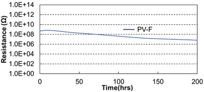
| Insulation Reliability | Layer to layer 130 ℃, 85 %RH, 5.5 V, 15 µm |
200hr Pass |
* Available upon request for film thickness
Various pattern images (thickness : 25 µm)

Layer to layer insulation reliability
Test condition; 130 ℃, 85 %RH, 5.5 V
Test coupon image

Test results graph

