Base Materials for PWBs
Halogen Free, High Tg, High Elastic Modulus, Low CTE Multilayer Material – MCL-E-705G
Product Information and Application
Product form
- CCL: MCL-E-705G
- Prepreg: GEA-705G
Applications
- Semiconductor packages. (FC-BGA, FC-CSP, PoP, SiP)
- HDI, PWB
- Thinner module, PWB
Features
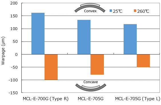
- MCL-E-705G has low CTE values in X, Y directions and reduces warpage of package substrate significantly.
- MCL-E-705G (Type L) has lower CTE value (≤5ppm/℃).
- MCL-E-705G (Type LH) has lower CTE value (3ppm/℃).
- Well-suited for build-up construction.
Characteristics
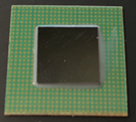
Warpage of FC-BGA

TEG Chip
- Chip size: 20mm×20mm
- Chip thickness: 0.725mm
- Bump diameter: 80 µm
- Bump pitch: 200 µm
TEG Substrate
- Package size: 35mm×35mm
- Core thickness: 0.4mm
- Build up thickness: 30 µm×2stack
- SR thickness: 20 µm
Warpage of PKG

TEG Substrate Spec
- Size: 14mm×14mm
- Total thickness: 250 µm
- SR thickness: 20 µm (SR-7200G: Showa Denko Materials)
- Prepreg thickness: 40 µm
- Core thickness: 110 µm

Thin Laminate
(t0.4mm)
| Item | Condition *3 | Unit | Actual Value | Reference | |||||
|---|---|---|---|---|---|---|---|---|---|
| MCL-E- 705G |
MCL-E- 705G (Type X) |
MCL-E- 705G (Type L) |
MCL-E- 705G (Type LH) |
(IPC-TM-650) | |||||
| Tg | TMA method | A | ℃ | 250–270 | 2.4.24 | ||||
| DMA method | A | 295–305 | ‐ | ||||||
| CTE *1 | X (30–120℃) | A | ppm/℃ | 5–7 | 4–6 | 3–4 | 2.5–3.5 | ‐ | |
| Y (30–120℃) | A | 5–7 | 4–6 | 3–4 | 2.5–3.5 | ||||
| Z*4 | (<Tg) | A | 10–15 | 2.4.24 | |||||
| (>Tg) | 70–100 | ||||||||
| Solder Heat Resistance (260℃) | A | sec. | >300 | ‐ | |||||
| T-260 (Without Copper) | A | min. | >60 | 2.4.24.1 | |||||
| T-288 (Without Copper) | A | >60 | |||||||
| Decomposition Temperature (TGA method 5% Weight Loss) | A | ℃ | 430–450 | 2.3.40 | |||||
| Heat Resistance for HDI Process (Semi-Additive) | 260℃ Reflow | cycles | >20 | ‐ | |||||
| Copper Peel Strength | 12 µm | A | kN/m | 0.8–1.0 | 2.4.8 | ||||
| 18 µm | A | 0.9–1.1 | |||||||
| Surface Roughness (Ra) | A | µm | 2–3 | 2.2.17 | |||||
| Flexural Modulus (Lengthwise) *4 | A | GPa | 32–34 | 33–35 | 34–36 | 37–39 | ‐ | ||
| Dielectric Constant | 10GHz *2 | A | ‐ | 4.4–4.6 | 4.4–4.6 | 4.1–4.3 | 4.1–4.3 | IEC-61189-2-721 | |
| Dissipation Factor | 10GHz *2 | A | ‐ | 0.009–0.011 | IEC-61189-2-721 | ||||
| Volume Resistivity | C-96/40/90 | Ω・cm | 1×10¹⁴–1×10¹⁶ | 2.5.17 | |||||
| Surface Resistance | C-96/40/90 | Ω | 1×10¹³–1×10¹⁵ | ||||||
| Insulation Resistance | A | Ω | 1×10¹⁴–1×10¹⁶ | ‐ | |||||
| D-2/100 | 1×10¹²–1×10¹⁴ | ‐ | |||||||
*1) Heating Rate: 10℃/min., *2) Measured by SPDR., *3) Refer to “Condition Note“, *4) t0.8mm
*Above data are experimental results and not guaranteed.
Standard Specifications
Copper Clad Laminate
| Part Number | Type | Copper Foil Thickness | Thickness Code | Laminate Thickness |
|---|---|---|---|---|
| MCL-E- 705G |
– (L) |
2 µm, 3 µm, 12 µm (LP, PF) | T0.06 | 0.06mm |
| 12 µm 18 µm (STD) 2 µm 3 µm 12 µm (LP, PF) |
M0.06 | 0.06mm | ||
| 0.1 | 0.11mm | |||
| M0.11 | 0.10mm | |||
| M0.15 | 0.16mm | |||
| M0.22 | 0.21mm | |||
| 0.2 | 0.21mm | |||
| 0.31 | 0.31mm | |||
| 0.41 | 0.41mm | |||
| 0.51 | 0.52mm | |||
| 0.61 | 0.62mm | |||
| 0.71 | 0.72mm | |||
| 0.81 | 0.82mm | |||
| (X) | 12 µm 18 µm (STD) 2 µm 3 µm 12 µm (LP, PF) |
0.41 | 0.41mm | |
| 0.61 | 0.62mm | |||
| 0.81 | 0.82mm | |||
| (LH) | M0.06 | 0.06mm | ||
| 0.1 | 0.11mm | |||
| D0.15 | 0.16mm | |||
| 0.2 | 0.21mm | |||
| 0.26 | 0.26mm |
Note1) STD: Standard copper foil, LP: Low profile copper foil, PF: Hitachi profile-free copper foil.
Note2) STD: 12 µm, 18 µm; LP: 2 µm, 3 µm, 12 µm, 18 µm; PF:2 µm, 3 µm, 12 µm.
Note3)“U” for 1-ply“; T” for 2-ply.
Note4) The thickness means that of dielectric layer.
Prepreg
| Part Number | Type | Glass Cloth | Properties | |||
|---|---|---|---|---|---|---|
| Style | Resin Content (%) |
Dielectric Thickness after Lamination *1 (mm) |
||||
| GEA-705G | (F) | ≦0.025 | (See [GEA-705G (Type F)]page for ultra thin, flat prepregs) | |||
| ‐ | 0.025 | (1017N73) | 1017 | 73±2 | 0.025 | |
| 0.03 | (1027N73) | 1027 | 73±2 | 0.040 | ||
| 0.04 | (1037N73) | 1037 | 73±2 | 0.048 | ||
| 0.06 | (1078N65) | 1078 | 65±2 | 0.071 | ||
| 0.1 | (2116N58) | 2116 | 58±2 | 0.126 | ||
| (L) | 0.025 | (L1017N73) | 1017 | 73±2 | 0.025 | |
| 0.03 | (L1027N73) | 1027 | 73±2 | 0.040 | ||
| 0.04 | (L1037N73) | 1037 | 73±2 | 0.048 | ||
| 0.06 | (L1078N65) | 1078 | 65±2 | 0.071 | ||
| 0.1 | (L2116N58) | 2116 | 58±2 | 0.126 | ||
| Reference (IPC-TM-650) | 2.3.16 | ‐ | ||||
*1) The dielectric thickness after lamination is defined as the thickness of one sheet of prepreg when the resin flow is 0%.
This value changes depending on the press condition or inner layer pattern.
