Base Materials for PWBs
Copper Foil for Fine Patterning – PF-EL
Product Information and Application
Product form
- Copper Foil: PF-EL
Applications
- Semiconductor package substrates
- High density multi-layer PWB
Features
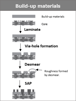
- PF-EL is a copper foil that is appropriate for fine line patterning with semi-additive process (SAP) using rough shapes of primer made with the copper profile.
- PF-EL has high peel strength for plating copper.
- High flexural modulus substrates with using prepregs.
Characteristics
Surface
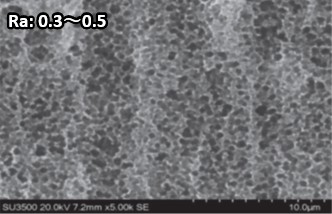
PF-EL
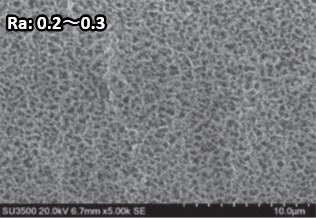
PF-EL SP
Fine patterning with SAP
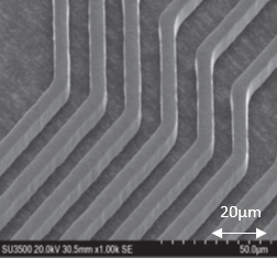
Design
L/S=10/10 µm with PF-EL
(Exposure LDⅠ)
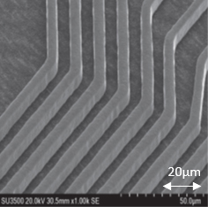
Design
L/S=7/7 µm with PF-EL SP
(Exposure LDⅠ)
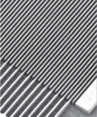
Design
L/S=5/5 µm with PF-EL SP
(Exposure Stepper)
Copper peel strength
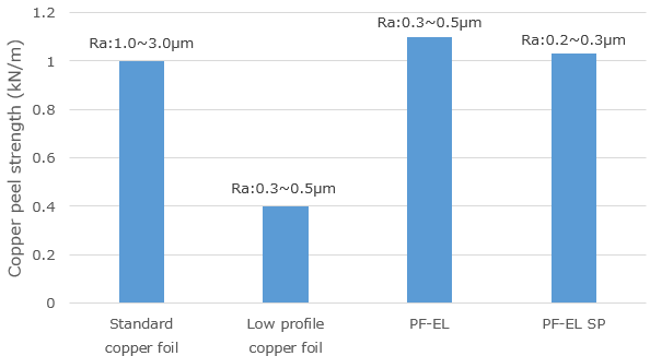
*Sample: MCL-E-770G (Type R), Copper foil 1.5 µm with plating copper 20 µm
Plating copper peel strength
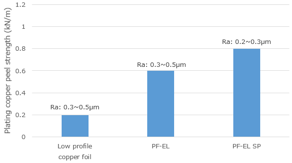
*Sample: MCL-E-770G (Type R), plating copper 20 µm
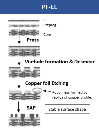
Fine patterning process
Standard Specifications
Copper Foil
| Part Number | Copper Foil Thickness (µm) |
Special Surface Treatment (µm) |
Roughness (µm) | Composition | Process |
|---|---|---|---|---|---|
| PF-EL-12 | 12 | 4 | Ra: 0.3–0.4 | 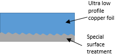 |
SAP *1 |
| Rz: 1.5–2.5 | |||||
| PF-EL-3 | 3 | 2, 4 | Ra: 0.3–0.5 | SAP *1 MSAP *2 |
|
| Rz: 1.5–2.5 | |||||
| PF-EL-2 | 2 | 2, 4 | Ra: 0.3–0.5 | ||
| Rz: 1.5–2.5 | |||||
| PF-EL-1.5 | 1.5 | 2 | Ra: 0.3–0.5 | ||
| Rz: 1.5–2.5 | |||||
| PF-EL-1.5SP | 1.5 | 2 | Ra: 0.2–0.3 | ||
| Rz: 1.0–2.0 |
*1) After lamination of the material to the prepreg, the copper foil is etched out,and the special surface treatment with appropriate roughness made by a replica of the copper profile etched out remains on prepreg surface.This process is SAP using this replica.
*2) Semi additive process using thin copper foil as seed layer for having E’less copper +copper on both patterming and via plating purpose.
