Base Materials for PWBs
Halogen Free, High Elastic Modulus, Low CTE Multilayer Material – MCL-E-679FG
Product Information and Application
Product form
- CCL: MCL-E-679FG, MCL-E-679FGB 〈Black Type〉
- Prepreg: GEA-679FG
Applications
- Semiconductor packages. (FC-BGA, BGA, CSP)
- Build up PWB.
- Personal computer, high density electronic equipment.
Features
- Halogen free material for environmental concerns.
- CTE (Z-direction) is 50% lower than that of our standard FR-4.
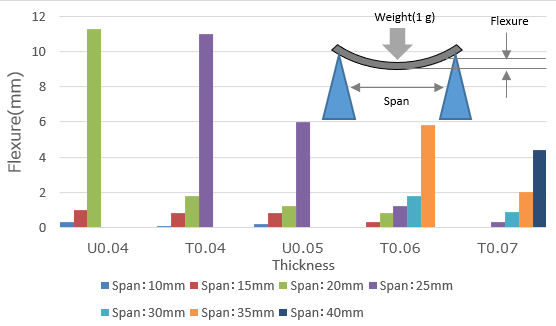
- Elastic modulus is 20% higher than that of our standard FR-4. Even thin laminate has less warpage and deflection.
- Superior heat resistance for soldering (suitable for lead free process).
- Suitable for fine patterning with 1/4 surface roughness of our standard FR-4 pattern possible.
Characteristics
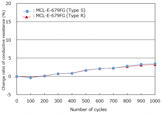
Through-hole reliability
Test condition: -55℃, 30min. ⇔150℃, 30min.
Pattern: Wall to wall distance 0.3mm, Laminate thickness: t0.8mm
Pre-condition: 260℃ reflow × 2times⇒Solder dipping (260℃ 10sec.)

Stiffness Properties

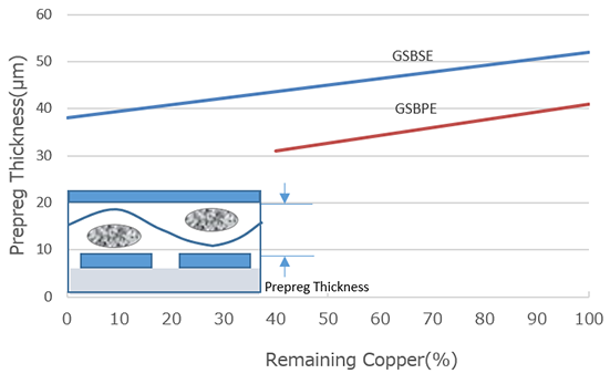
Prepreg thickness after pattern filling (Inner layer copper 15 µm)

Thin Laminate
| Item | Condition *3 | Unit | Actual Value | Reference (IPC-TM-650) |
|||||
|---|---|---|---|---|---|---|---|---|---|
| MCL-E- 679FGB (Type R) |
MCL-E- 679FG (Type R) |
MCL-E- 679FGB (Type S) |
MCL-E- 679FG (Type S) |
||||||
| Tg | TMA method | A | ℃ | 165–175 | 175–185 | 2.4.24 | |||
| DMA method | A | 200–220 | 210–230 | ‐ | |||||
| CTE *1 | X (30–120℃) | A | ppm/℃ | 13–15 | 12–14 | ‐ | |||
| Y (30–120℃) | A | 13–15 | 12–14 | ||||||
| Z | (<Tg) | A | 23–33 | 20–30 | 2.4.24 | ||||
| (>Tg) | 140–170 | 130–160 | |||||||
| Solder Heat Resistance (260℃) | A | sec. | >300 | ‐ | |||||
| T-260 (Without Copper) | A | min. | >60 | 2.4.24.1 | |||||
| T-288 (Without Copper) | A | >60 | |||||||
| Decomposition Temperature (TGA method 5% Weight Loss) | A | ℃ | 340–360 | 2.3.40 | |||||
| Heat Resistance for HDI Process | 260℃ Reflow | cycles | >10 | ‐ | |||||
| Copper Peel Strength | 18 µm | A | kN/m | 0.9–1.1 | 1.1–1.2 | 2.4.8 | |||
| 35 µm | A | 1.1–1.2 | 1.2–1.3 | ||||||
| Surface Roughness (Ra) | A | µm | 2–3 | 2.2.17 | |||||
| Flexural Modulus (Lengthwise) | A | GPa | 23–28 | 24–29 | ‐ | ||||
| Dielectric Constant | 1GHz *2 | A | ‐ | 4.9–5.1 | ‐ | ||||
| 10GHz *2 | 4.8–5.0 | ‐ | |||||||
| Dissipation Factor | 1GHz *2 | A | ‐ | 0.013–0.015 | ‐ | ||||
| 10GHz *2 | 0.014–0.016 | ‐ | |||||||
| Volume Resistivity | C-96/40/90 | Ω・cm | 1×10¹⁴–1×10¹⁶ | 2.5.17 | |||||
| Surface Resistance | C-96/40/90 | Ω | 1×10¹³–1×10¹⁵ | ||||||
| Insulation Resistance | A | Ω | 1×10¹⁴–1×10¹⁶ | ‐ | |||||
| D-2/100 | 1×10¹²–1×10¹⁴ | ‐ | |||||||
*1) Heating Rate: 10℃/min., *2) Measured by SPDR method., *3) Refer to “Condition Note”
*Above data are experimental results and not guaranteed.
Standard Specifications
Copper Clad Laminate
| Part Number | Type | Copper Foil Thickness | Code Name | Laminate Thickness |
|---|---|---|---|---|
| MCL-E-679FG MCL-E-679FGB |
(S) | 3 µm | U0.03 | 0.030mm |
| U0.04 | 0.040mm | |||
| U0.05 | 0.050mm | |||
| T0.04 | 0.040mm | |||
| T0.06 | 0.060mm | |||
| 3, 12, 18 µm (STD, LP) |
T0.07 | 0.070mm | ||
| M0.06 | 0.07mm | |||
| (R) (S) |
3 µm 12 µm 18 µm, 35 µm (STD, LP) |
0.1 | 0.11mm | |
| 0.2 | 0.20mm | |||
| 0.41 | 0.40mm | |||
| 0.81 | 0.80mm |
Note1) STD: Standard copper foil, LP: Low profile copper foil,
Note2) STD: 12 µm, 18 µm, 35 µm; LP: 3 µm, 12 µm, 18 µm.
Note3) “U” for 1-ply“; T” for 2-ply.
Note4) The thickness means that of dielectric layer.
Prepreg
| Part Number | Type | Glass Cloth | Properties | |||
|---|---|---|---|---|---|---|
| Style | Resin Content (%) |
Dielectric Thickness after Lamination *1 (mm) |
||||
| GEA-679FG *2 | (R) | 0.03 | (GBPE) | 1027 | 73±2 | 0.040 |
| 0.04 | (GRZPE) | 1037 | 73±2 | 0.048 | ||
| 0.06 | (GRROE) | 1078 | 68±2 | 0.079 | ||
| 0.1 | (GRSKE) | 2116 | 58±2 | 0.127 | ||
| (S) | 0.03 | (GSBPE) | 1027 | 73±2 | 0.040 | |
| 0.03 | (GSBSE) | 1027 | 78±2 | 0.050 | ||
| 0.04 | (GSZPE) | 1037 | 73±2 | 0.048 | ||
| 0.06 | (GSROE) | 1078 | 68±2 | 0.079 | ||
| 0.1 | (GSSKE) | 2116 | 58±2 | 0.127 | ||
| Reference (IPC-TM-650) | 2.3.16 | ‐ | ||||
*1) The dielectric thickness after lamination is defined as the thickness of one sheet of prepreg when the resin flow is 0%.
This value changes depending on the press condition or inner layer pattern.
*2) Black type is not available for prepreg.
